The printed circuit board (PCB) design and manufacturing process is an intricate one that requires careful consideration of many components to ensure success. To create a successful PCB, engineers must take into account the type of materials used, the electrical pathways needed for proper functioning, and other factors such as cost-effectiveness and manufacturability.
This article will provide an overview of all aspects related to PCB design and manufacturing so that readers can gain a better understanding of this complex process.
Introduction to PCB Design and Manufacturing
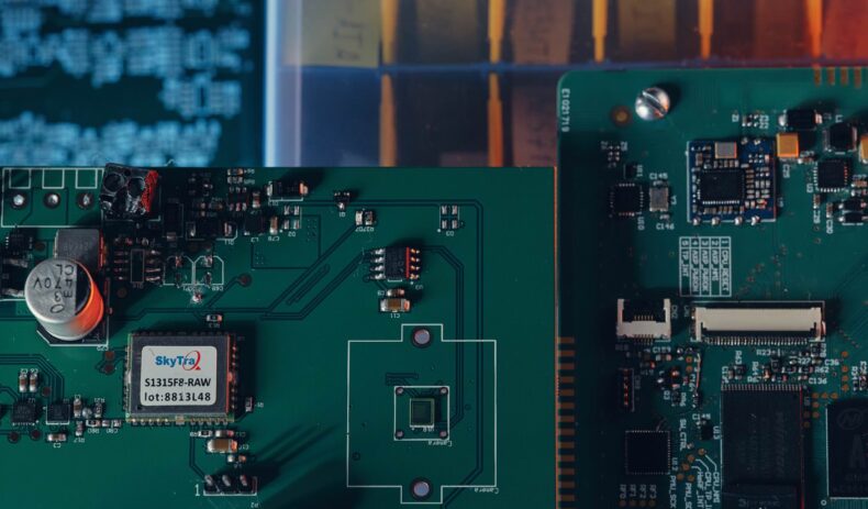
PCB design and manufacturing is an essential process in the creation of modern electronics. It involves taking a schematic, which is essentially a blueprint for the electrical components on the board, and turning it into reality.
This requires careful consideration of component placement, trace routing, power delivery systems, testing strategies, and more. The goal of this overview is to provide readers with an understanding of how these processes work together so that they can make informed decisions when designing their products.
We will look at each step in turn from concept to completion as well as common mistakes that could lead to costly errors down the line.
Design Process Overview
Source: www.autodesk.com
The design process overview for PCB design and manufacturing is an essential part of the production cycle. It involves several steps that must be taken to ensure the best possible outcome from your project.
The first step is to develop a schematic diagram, which will serve as a blueprint for the board layout. This should include all components, their connections, and other necessary information such as physical dimensions and component placement.
Next, you must create three-dimensional models of each element on the board so that they can be accurately placed on the board during fabrication. Once this is done, you can move on to creating artwork files which are used by manufacturers to produce exactly what you have designed with minimal mistakes or errors.
Finally, after everything has been tested and approved, it is time for fabrication – when all components are assembled into one cohesive unit before being shipped off to its final destination!
Manufacturing Process Overview
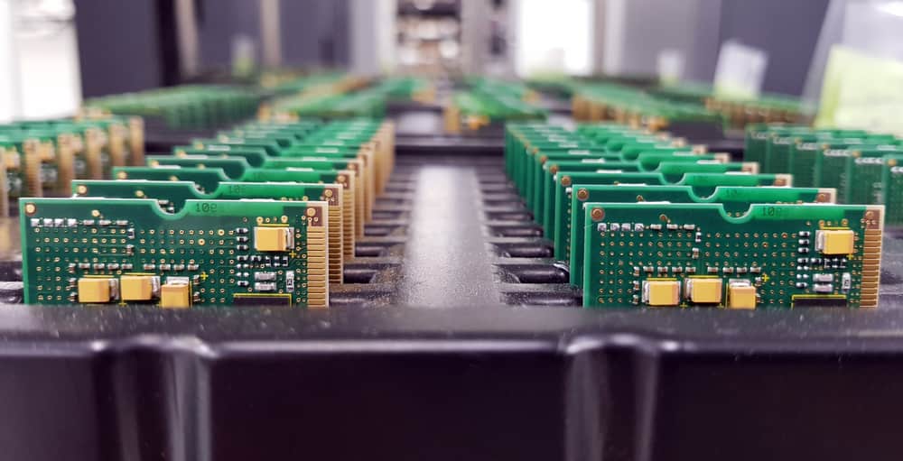
The manufacturing process of a PCB is complex and multifaceted. It involves multiple stages, from designing the board to ordering components to performing assembly and testing.
During the design stage, engineers create a schematic that outlines the electrical connections for each component on the board. After this, they will generate an electronic layout diagram that details where each component should be placed on the board to meet its specific requirements.
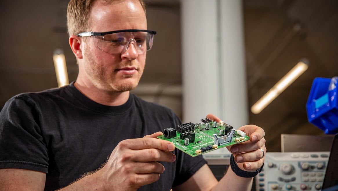
Once approved by customers or engineers, both digital and physical prototypes are created using specialized machines such as 3D printers or CNC routers. During the production phase, components are purchased from suppliers and then sorted according to their type before being attached to pre-made boards with through-hole technology or surface mount technology (SMT). Automated pick-and-place machines can also be used at this stage if needed.
Then all soldered points are inspected under microscopes for any defects before proceeding further into the testing phase. Components must pass tests such as temperature cycling tests while circuit boards must pass tests involving power supplies, voltage levels checks, etc.
, before shipment out of factory premises for them to perform up to standard when used by end users afterward.
Quality Control and Testing Procedures
Source: wevolver.com
Quality control and testing procedures are essential components of the PCB design and manufacturing process. Before a completed board is ready for use, it must go through rigorous tests to ensure that all specifications are met.
This includes electrical testing such as functional verification tests, in-circuit testing, boundary scan tests, signal integrity checks, EMC/EMI compliance measurements, and more. Additionally, visual inspections may be carried out to check for any defects or irregularities on the surface of the board.
If any issues are detected during these tests then they must be addressed before production can proceed further. The quality control team also has the responsibility of validating that each step in the production process was executed correctly according to predetermined standards set by industry professionals.
By regularly performing comprehensive quality checks throughout every stage of PCB design and manufacture, manufacturers can guarantee their products will meet customer requirements while ensuring safety and reliability at all times.
Conclusion
The Printed Circuit Board (PCB) design and manufacturing process is an intricate one, requiring a great deal of expertise and attention to detail. From the schematic design phase to board layout and fabrication, every step must be done with precision for the PCB to function as intended.
The manufacture of a successful PCB requires both technical knowledge as well as creative problem-solving skills. With careful planning and execution, a high-quality PCB can be designed that meets the unique needs of each project.
By understanding all aspects of the PCB design process, engineers can confidently create reliable circuit boards that are suitable for their application.
Source: tronicszone.com


